 |
| 10 Helpful PCB Assembly Tips for Product Developers |
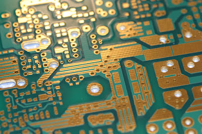
PCB (Printed Circuit Board) is a basic thing in any electronic circuit. The whole board is responsible for communication between different components. The product developers are a final step of product design but avoiding some steps can lead to serious problems. Assembling requires some special steps to follow. These steps are common in designing and developing PCB but the developer’s intention is required to these steps. Otherwise, the issues are formable easily. The components on the PCB needs to attach with specific measurement and protocols. To assemble every component the PCB developers, need to focus on some points:
1. Consulting with Designer
There are different kinds of companies for PCB designing with assembling. Every company should communicate with its buyer from the start, even before PCB designing. Almost every company which offers the PCB assembling also designs the PCBs. Some buyers prefer to make it from their selective Designers. In those cases when the Designer is from within or outside the company, he/she should get the guideline from its developer. Especially for which component developers have and which he prefers to use. In that case, the assembling process becomes easy and assembler doesn’t have to struggle for available components.
 |
| 10 Helpful PCB Assembly Tips for Product Developers |
2. VIAS
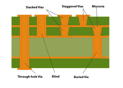
In every PCB, the Developer will get vias that are used to connect the different layers for proper path. The larger number of vias aren’t good for PCB. They are alike drill points on the PCB but their basic purpose is the connection within layers. Before starting the assembling of components on the PCB try to fill out the vias otherwise, it could cause confusion between the components drill points and itself.
 |
| 10 Helpful PCB Assembly Tips for Product Developers |
3. COMPONENTS GUIDELINES
In the case of handmade assembling, Every PCB Designers provide the silkscreen on the PCB for each component placement. In some cases, PCB loses its silkscreen for some components. The only way to make it clear for each component use the 3d model of the PCB design, which can be generated through any PCB designing software.
 |
| 10 Helpful PCB Assembly Tips for Product Developers |
4. SMART SELECTION & PLACEMENT
To start the assembling collect all the components from the BOM file. The components’ collection will be a major step and should be from the BOM file otherwise it could cause problems later. The components come from different manufacture with internal design. Try to select the less heat producer and cheap components. This will help in reducing costs and make the PCB efficient. Sometimes the lowering the cost could cause a lowering in quality. So, always contact the buyer and focus on his intention’s requirements. The placement of components smartly can also solve multiple issues.
 |
| 10 Helpful PCB Assembly Tips for Product Developers |
5. SMD/SMT COMPONENTS
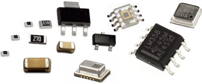
Whenever the PCB has only SMD components then start from the smaller ones. In SMD components the 0602 model of the components is preferable due to their average size. The other components are also useable but the model 0602 and larger than itself are best for PCB.
 |
| 10 Helpful PCB Assembly Tips for Product Developers |
6. THT COMPONENTS
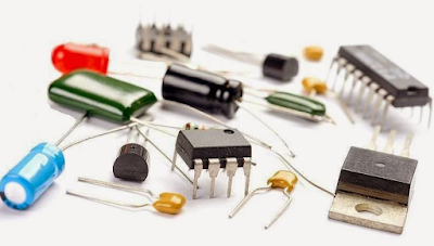
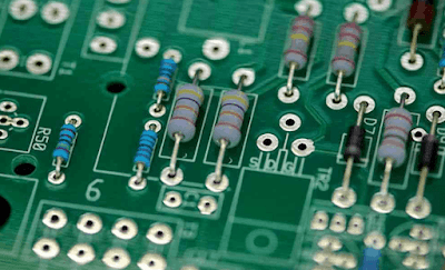
Some PCB with high load only contains THT Components. In that case, the components need to place on a single side. The use of a single layer is only possible in THT components only because of their drilled connection. The components on the single side will make the PCB safer and its height will also become lower and manageable. Try to place the smaller sized components first in the THT placement. In THT the components could overlap easily. The problem can be avoided by changing the layer of the component. If it can’t be avoided then try proper protection between overlapped components.
 |
| 10 Helpful PCB Assembly Tips for Product Developers |
7. PLACEMENT OF Mixed Components
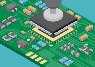
In-circuit boards most of the components could be SMD/SMT. To start the assembling of PCB the SMD components need to place first on the PCB. The SMD components will have a smaller size, and they will be hard to connect when THT components are already been placed. Both SMD and THT components are Larger size components. In PCB assembling try to start from the small components and then move towards the larger components. In case of larger component keep moving from the center towards the border. Even if it is possible, try to talk with the designer for placing the larger components at the border. This will save the pick and place the time of the developers.
 |
| 10 Helpful PCB Assembly Tips for Product Developers |
8. HEAT PROBLEM
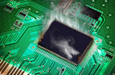
The heating factor is one of the problematic factors for PCB. The excessive heat-producing components should not interact with each other and need to place far away from each other. They could harm other components just by excessive heat. This issue comes mostly in THT components and also forgets the single-layer tip for that case.
 |
| 10 Helpful PCB Assembly Tips for Product Developers |
9. SOLDERING
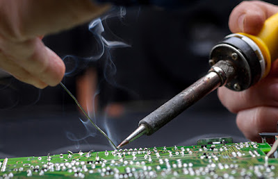
It is the final step in the PCB assembling for developers. In soldering first, try to use the minimum solder as much you can. This will help in reducing heat and short circuit between components. During soldering avoid pad share and heat interaction between components. Therefore, always place the component where it has been marked by the Designer. Heat interaction from kavia could burn some components easily.
 |
| 10 Helpful PCB Assembly Tips for Product Developers |
10. SOLUTIONS OF MISTAKES
First, try to avoid mistakes in attaching components. Even, if you made a mistake then don’t try to use the force to remove the components. Try to use the proper equipment to solve any mistake. If you don’t have specific equipment for mistakes you have done then solve them with a proper protocol. Just try to avoid the use of force on the PCB. This could disconnect the trace of the PCB which can be costly.
Sometimes the connections between components and PCB feel connected but in reality, they aren’t connected. To avoid this mistake, try to verify them after their assembling. The final problem most of the PCB creates is that the remains of solder or the small wires on the PCB or between the component, which can cause problems. Try to avoid it, otherwise short circuits can happen and the whole PCB could become waste with its components.
The above 10 tips won’t only solve the Assembling issue developers face normally; it will also help them to design the best PCB for your buyer with lower cost and timely.
Post a Comment